Revision as of 11:19, 8 January 2011 by imported>John R. Brews
I am a Professor Emeritus of Electrical Engineering from The University of Arizona, where I taught device physics and circuit design for just under two decades. Previously, I was a research scientist for twenty-odd years at Bell Laboratories, Murray Hill, doing theoretical work in the areas of solid-state physics and device physics. I also am a Fellow of the IEEE, and a recipient of the Electron Device Society distinguished service award for work as Editor-in-chief of the journal IEEE Electron Device Letters, founded by Nobel prize winner George E. Smith. I've published a number of technical books and papers, some of which may be found at this link.
Images
| Magnetism
|
|
|
(CC) Image: John R. Brews
|
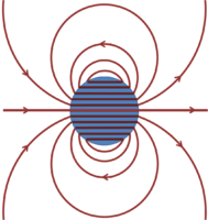
B-field lines near uniformly magnetized sphere
|
|
|
(CC) Image: John R. Brews
|
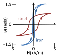
Magnetic flux density vs. magnetic field in steel and iron
|
|
| Widlar current source
|
|
|
(CC) Image: John R. Brews
|
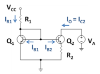
Widlar current source using bipolar transistors
|
|
|
(CC) Image: John R. Brews
|
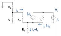
Small-signal circuit for finding output resistance of the Widlar source
|
|
|
(CC) Image: John R. Brews
|
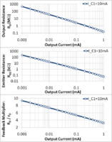
Design trade-off between output resistance and output current in Widlar source
|
|
| Forces
|
|
|
(CC) Image: John R. Brews
|
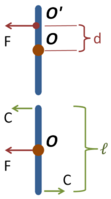
Force and its equivalent force and couple
|
|
| Electromagnetism
|
|
|
(CC) Image: John R. Brews
|
|
|
|
| Devices
|
|
|
(PD) Image: John R. Brews
|
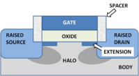
A modern MOSFET
|
|
|
(CC) Image: John R. Brews
|
Calculated density of states for crystalline silicon.
|
|
|
(CC) Image: John R. Brews
|
A narrow, surface inversion layer of electrons forms at large enough positive gate voltages. The horizontal dashed line indicates the Fermi level that divides occupied energy levels from empty ones at zero temperature.
|
|
|
(PD) Image: John R. Brews
|
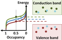
Occupancy comparison between n-type, intrinsic and p-type semiconductors.
|
|
