Revision as of 23:16, 15 February 2011 by imported>John R. Brews
I am a Professor Emeritus of Electrical Engineering from The University of Arizona, where I taught device physics and circuit design for just under two decades. Previously, I was a research scientist for twenty-odd years at Bell Laboratories, Murray Hill, doing theoretical work in the areas of solid-state physics and device physics. I also am a Fellow of the IEEE, and a recipient of the Electron Device Society distinguished service award for work as Editor-in-chief of the journal IEEE Electron Device Letters, founded by Nobel prize winner George E. Smith. I've published a number of technical books and papers, some of which may be found at this link.
Images
| Magnetism
|
|
|
(CC) Image: John R. Brews
|
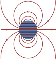
B-field lines near uniformly magnetized sphere
|
|
|
(CC) Image: John R. Brews
|
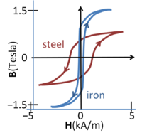
Magnetic flux density vs. magnetic field in steel and iron
|
|
| Widlar current source
|
|
|
(CC) Image: John R. Brews
|
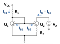
Widlar current source using bipolar transistors
|
|
|
(CC) Image: John R. Brews
|
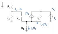
Small-signal circuit for finding output resistance of the Widlar source
|
|
|
(CC) Image: John R. Brews
|
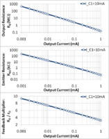
Design trade-off between output resistance and output current in Widlar source
|
|
| Forces
|
|
|
(CC) Image: John R. Brews
|
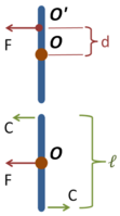
Force and its equivalent force and couple
|
|
|
(PD) Image: John R. Brews
|
Centripetal force FC upon an object held in circular motion by a string of length R. The string is under tension FT, as shown separately to the left.
|
|
|
(PD) Image: John R. Brews
|
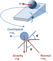
Upper panel: Ball on a banked circular track moving with constant speed v; Lower panel: Forces on the ball.
|
|
|
(PD) Image: John R. Brews
|
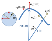
Polar unit vectors at two times t and t + dt for a particle with trajectory r ( t ); on the left the unit vectors uρ and uθ at the two times are moved so their tails all meet, and are shown to trace an arc of a unit radius circle.
|
|
|
(PD) Image: John R. Brews
|
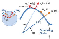
Local coordinate system for planar motion on a curve.
|
|
|
(PD) Image: John R. Brews
|
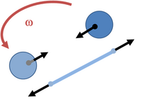
Exploded view of rotating spheres in an inertial frame of reference showing the centripetal forces on the spheres provided by the tension in a rope tying them together.
|
|
|
(PD) Image: John R. Brews
|
Rotating spheres subject to centrifugal (outward) force in a co-rotating frame in addition to the (inward) tension from the rope.
|
|
|
(PD) Image: John R. Brews
|
The "whirling table". The rod is made to rotate about the axis and (from the bead's viewpoint) the centrifugal force acting on the sliding bead is balanced by the weight attached by a cord over two pulleys.
|
|
|
(PD) Image: John R. Brews
|
Force diagram for an element of water surface in co-rotating frame.
|
|
|
(PD) Image: John R. Brews
|
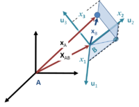
An object located at xA in inertial frame A is located at location xB in accelerating frame B.
|
|
|
(PD) Image: John R. Brews
|
An orbiting but fixed orientation coordinate system B, shown at three different times.
|
|
|
(PD) Image: John R. Brews
|
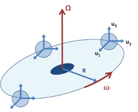
An orbiting coordinate system B in which unit vectors uj, j = 1, 2, 3 rotate to face the rotational axis.
|
|
| Electromagnetism
|
|
|
(CC) Image: John R. Brews
|
|
|
|
| Devices
|
|
|
(PD) Image: John R. Brews
|
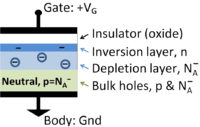
Cross section of MOS capacitor showing charge layers
|
|
|
(PD) Image: John R. Brews
|
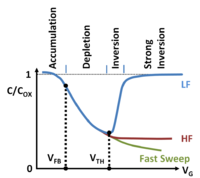
Three types of MOS capacitance vs. voltage curves. VTH = threshold, VFB = flatbands
|
|
|
(PD) Image: John R. Brews
|
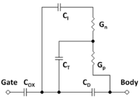
Small-signal equivalent circuit of the MOS capacitor in inversion with a single trap level
|
|
|
(PD) Image: John R. Brews
|
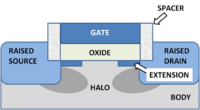
A modern MOSFET
|
|
|
(PD) Image: John R. Brews
|
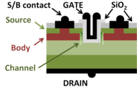
A power MOSFET; source and body share a contact.
|
|
|
(CC) Image: John R. Brews
|
Calculated density of states for crystalline silicon.
|
|
|
(CC) Image: John R. Brews
|
Field effect: At a gate voltage above threshold a surface inversion layer of electrons forms at a semiconductor surface.
|
|
|
(PD) Image: John R. Brews
|
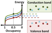
Occupancy comparison between n-type, intrinsic and p-type semiconductors.
|
|
|
(PD) Image: John R. Brews
|
Nonideal pn-diode current-voltage characteristics
|
|
|
(PD) Image: John R. Brews
|
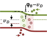
Band-bending diagram for pn-junction diode at zero applied voltage
|
|
|
(PD) Image: John R. Brews
|
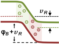
Band-bending for pn-diode in reverse bias
|
|
|
(PD) Image: John R. Brews
|
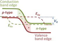
Quasi-Fermi levels in reverse-biased pn-junction diode
|
|
|
(PD) Image: John R. Brews
|
Band-bending diagram for pn-diode in forward bias
|
|
|
(PD) Image: John R. Brews
|
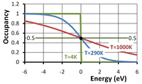
Fermi occupancy function vs. energy departure from Fermi level in volts for three temperatures
|
|
|
(PD) Image: John R. Brews
|
Fermi surface in k-space for a nearly filled band in the face-centered cubic lattice
|
|
|
(PD) Image: John R. Brews
|
A constant energy surface in the silicon conduction band consists of six ellipsoids.
|
|
|
(PD) Image: John R. Brews
|
Planar Schottky diode with n+-guard rings and tapered oxide.
|
|
|
(PD) Image: John R. Brews
|
Comparison of Schottky and pn-diode current voltage curves.
|
|
|
(PD) Image: John R. Brews
|
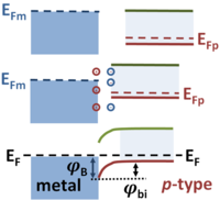
Schottky barrier formation on p-type semiconductor. Energies are in eV.
|
|
|
(PD) Image: John R. Brews
|
Schottky diode under forward bias VF.
|
|
|
(PD) Image: John R. Brews
|
Schottky diode under reverse bias VR.
|
|
|
(PD) Image: John R. Brews
|
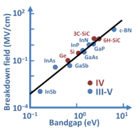
Critical electric field for breakdown versus bandgap energy in several materials.
|
|
|
(PD) Image: John R. Brews
|
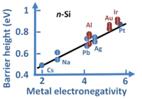
Schottky barrier height vs. metal electronegativity for some selected metals on n-type silicon.
|
|
