Bipolar transistor: Difference between revisions
imported>John R. Brews m (→Output resistance rO: edit link) |
mNo edit summary |
||
| (2 intermediate revisions by 2 users not shown) | |||
| Line 4: | Line 4: | ||
{{Image|Planar bipolar transistor.PNG|right|200px|A planar ''npn'' bipolar junction transistor as might be constructed in a [[integrated circuit]].}} | {{Image|Planar bipolar transistor.PNG|right|200px|A planar ''npn'' bipolar junction transistor as might be constructed in a [[integrated circuit]].}} | ||
In [[electronics]], the '''bipolar transistor''', more completely the '''bipolar junction transistor''', is a three terminal [[semiconductor|semiconductor device]] used for switching and amplification. In concept it consists of two back-to-back [[Semiconductor diode|''pn''-diodes]], forming either a ''pnp'' or an ''npn'' sandwich, where ''p'' refers to semiconductor doped to produce positively | In [[electronics]], the '''bipolar transistor''', more completely the '''bipolar junction transistor''', is a three-terminal [[semiconductor|semiconductor device]] used for switching and amplification. In concept it consists of two back-to-back [[Semiconductor diode|''pn''-diodes]], forming either a ''pnp'' or an ''npn'' sandwich, where ''p'' refers to a semiconductor doped to produce positively-charged carriers (holes) and ''n'' refers to a semiconductor doped to provide negatively-charged carriers (electrons). Moreover, the center region is thin enough to allow carriers injected from one of the end layers (the ''emitter'' ''E'') to actually ''diffuse'' across the center region (the ''base B'') and be collected by the other end region (the ''collector C''). | ||
Very small changes in the emitter-base junction voltage have an exponential influence over the number of carriers injected from the emitter, and so the base has enormous control over the current diffusing across the base to the collector. Moreover, the current consumed by the base in normal operation is very small, so the device serves well to amplify either a current or a voltage signal applied to the base. | Very small changes in the emitter-base junction voltage have an exponential influence over the number of carriers injected from the emitter, and so the base has enormous control over the current diffusing across the base to the collector. Moreover, the current consumed by the base in normal operation is very small, so the device serves well to amplify either a current or a voltage signal applied to the base. | ||
| Line 17: | Line 17: | ||
Using a [[band diagram]] as shown to the right, the operation can be understood. The diagram shows an npn transistor biased in active mode. It is a one-dimensional section vertically through the center of the emitter. The ''conduction band'' labeled ''CB'' shows the lowest energy of an electron (in electron volts, or energy divided by electron charge) in the conduction band of the semiconductor as a function of position in the npn transistor. The ''valence band'' labeled ''VB'' shows the highest energy for electrons in the semiconductor valence band. These two energy levels are separated by the semiconductor ''energy gap'', a region of forbidden energy for an electron. The ''CB'' and ''VB'' vary in position within the transistor for two reasons: variations in doping levels going from ''n-'' to ''p-'' to ''n-''type layers, and also variations in electrical potential through the structure. | Using a [[band diagram]] as shown to the right, the operation can be understood. The diagram shows an npn transistor biased in active mode. It is a one-dimensional section vertically through the center of the emitter. The ''conduction band'' labeled ''CB'' shows the lowest energy of an electron (in electron volts, or energy divided by electron charge) in the conduction band of the semiconductor as a function of position in the npn transistor. The ''valence band'' labeled ''VB'' shows the highest energy for electrons in the semiconductor valence band. These two energy levels are separated by the semiconductor ''energy gap'', a region of forbidden energy for an electron. The ''CB'' and ''VB'' vary in position within the transistor for two reasons: variations in doping levels going from ''n-'' to ''p-'' to ''n-''type layers, and also variations in electrical potential through the structure. | ||
If no bias is applied, the band edges vary because impurity atoms set the number of carriers, and the bands must adjust position to insure the correct carrier densities. The majority carrier [[Fermi level]]s in the various regions are shown as determined by the impurity dopant levels: ''E<sub>Fn<sub>'' for electrons in the field-free bulk of the emitter, ''E<sub>Fp<sub>'' for holes in the field free portion of the base, and ''E<sub>Fn<sub>'' for electrons in the field-free bulk of the collector. If the biases are reduced to zero, these Fermi levels all coincide. For more detail, see the | If no bias is applied, the band edges vary because impurity atoms set the number of carriers, and the bands must adjust position to insure the correct carrier densities. The majority carrier [[Fermi level]]s in the various regions are shown as determined by the impurity dopant levels: ''E<sub>Fn<sub>'' for electrons in the field-free bulk of the emitter, ''E<sub>Fp<sub>'' for holes in the field free portion of the base, and ''E<sub>Fn<sub>'' for electrons in the field-free bulk of the collector. If the biases are reduced to zero, these Fermi levels all coincide. For more detail, see the articles [[semiconductor]] and [[semiconductor diode]]. | ||
When bias is applied, the relative energies of the different regions are modified, upsetting equilibrium and causing the band edges to adjust in response. The Fermi levels are separated by the application of bias voltages across the junctions. The forward bias ''V<sub>BE</sub>'' splits the hole Fermi level in the base from the electron Fermi level in the emitter. Likewise, the reverse bias ''V<sub>CB</sub>'' splits the electron Fermi level in the bulk collector from the hole Fermi level in the field-free region of the base. | When bias is applied, the relative energies of the different regions are modified, upsetting equilibrium and causing the band edges to adjust in response. The Fermi levels are separated by the application of bias voltages across the junctions. The forward bias ''V<sub>BE</sub>'' splits the hole Fermi level in the base from the electron Fermi level in the emitter. Likewise, the reverse bias ''V<sub>CB</sub>'' splits the electron Fermi level in the bulk collector from the hole Fermi level in the field-free region of the base. | ||
| Line 120: | Line 120: | ||
{{cite book |title=Crystal fire: the birth of the information age |author=M Riordan & L Hoddeson |year=1997 |publisher=W. W. Norton & Company |url=http://books.google.com/books?id=0bTpcTLCu6MC&printsec=frontcover |isbn= 0393041247}} | {{cite book |title=Crystal fire: the birth of the information age |author=M Riordan & L Hoddeson |year=1997 |publisher=W. W. Norton & Company |url=http://books.google.com/books?id=0bTpcTLCu6MC&printsec=frontcover |isbn= 0393041247}} | ||
</ref> | </ref> | ||
}} | }}[[Category:Suggestion Bot Tag]] | ||
Latest revision as of 06:00, 19 July 2024

A planar npn bipolar junction transistor as might be constructed in a integrated circuit.
In electronics, the bipolar transistor, more completely the bipolar junction transistor, is a three-terminal semiconductor device used for switching and amplification. In concept it consists of two back-to-back pn-diodes, forming either a pnp or an npn sandwich, where p refers to a semiconductor doped to produce positively-charged carriers (holes) and n refers to a semiconductor doped to provide negatively-charged carriers (electrons). Moreover, the center region is thin enough to allow carriers injected from one of the end layers (the emitter E) to actually diffuse across the center region (the base B) and be collected by the other end region (the collector C).
Very small changes in the emitter-base junction voltage have an exponential influence over the number of carriers injected from the emitter, and so the base has enormous control over the current diffusing across the base to the collector. Moreover, the current consumed by the base in normal operation is very small, so the device serves well to amplify either a current or a voltage signal applied to the base.
History
The bipolar transistor was the historically first transistor invented. Prior to its invention in 1947 by Bardeen, Brattain and Shockley at Bell Laboratories, semiconductor devices were only two-terminal devices, like diodes and rectifiers. More of the history and development of this device can be found in an historical article by Shockley[1] and a more recent history.[2]
Operation
The bipolar transistor can operate in a number of modes, distinguished by which junctions are injecting (forward bias of emitter-base or collector-base or both) and which are collecting (reverse bias of emitter-base or collector base, or both). Here focus is upon the active mode in which the emitter-base junction is injecting and the collector-base junction is collecting. This mode is commonly used in analog circuits.
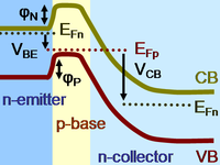
Using a band diagram as shown to the right, the operation can be understood. The diagram shows an npn transistor biased in active mode. It is a one-dimensional section vertically through the center of the emitter. The conduction band labeled CB shows the lowest energy of an electron (in electron volts, or energy divided by electron charge) in the conduction band of the semiconductor as a function of position in the npn transistor. The valence band labeled VB shows the highest energy for electrons in the semiconductor valence band. These two energy levels are separated by the semiconductor energy gap, a region of forbidden energy for an electron. The CB and VB vary in position within the transistor for two reasons: variations in doping levels going from n- to p- to n-type layers, and also variations in electrical potential through the structure.
If no bias is applied, the band edges vary because impurity atoms set the number of carriers, and the bands must adjust position to insure the correct carrier densities. The majority carrier Fermi levels in the various regions are shown as determined by the impurity dopant levels: EFn for electrons in the field-free bulk of the emitter, EFp for holes in the field free portion of the base, and EFn for electrons in the field-free bulk of the collector. If the biases are reduced to zero, these Fermi levels all coincide. For more detail, see the articles semiconductor and semiconductor diode.
When bias is applied, the relative energies of the different regions are modified, upsetting equilibrium and causing the band edges to adjust in response. The Fermi levels are separated by the application of bias voltages across the junctions. The forward bias VBE splits the hole Fermi level in the base from the electron Fermi level in the emitter. Likewise, the reverse bias VCB splits the electron Fermi level in the bulk collector from the hole Fermi level in the field-free region of the base.
The base-emitter junction is forward biased, that is, the base is made positive with respect to the emitter, attracting electrons. This forward bias VBE reduces the barrier φn that opposes entry of electrons into the base. Because the barrier is smaller, electrons enter the base, raising the concentration of electrons in the base above the normal equilibrium level and setting up a concentration gradient of electron density across the base. That gradient drives a diffusion current of electrons across the base (transport according to Fick's law of diffusion), toward the collector. At the same time, the collector is reverse biased by a voltage VCB with respect to the base, that is, made positive with respect to base, so it attracts electrons. This attraction reduces the electron density on the collector side of the base, adding to the gradient in electron density across the field-free portion of the base. The electrons diffusing across the base eventually reach the end of the field-free region, and enter the accelerating electric field created by the reverse bias on the collector. The transport of electrons then switches from diffusion due to the carrier gradient to drift under the action of the electric field.
The strong effect upon the collector current exerted by the base-emitter bias can be understood in terms of its large effect upon the electron density at the base-emitter interface. The number of electrons at the top of the barrier is a factor exp(−φn/Vth) smaller than the density in the emitter itself. Here Vth is the so-called thermal voltage given by:
where kB is the Boltzmann constant and T is the temperature in kelvins. At 290 K, Vth ≈ 25 mV. Thus, a change in this barrier height by an applied bias to become VBE smaller means the electron density at the top of the barrier becomes larger by a factor exp(VBE/Vth), a large exponential increase.
Using the same argument, the backward injection of holes from the base into the emitter also is increased by this same exponential factor. These holes recombine with electrons in the emitter and form a parasitic current consumption that must be supplied by the base current.
The heterojunction bipolar transistor attempts to reduce back injection of holes into the emitter by incorporating a wide bandgap emitter that will increase the barrier φp without increasing φn by changing the alignment of the valence bands of emitter and base without significant alteration of the conduction band alignment. Similarly, narrow bandgap base materials can reduce the electron barrier without reducing the hole barrier by realigning the conduction bands of emitter and base without significant change in the valence band alignment.[3]
Current gain β

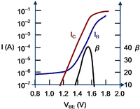
Gummel plot and current gain for a GaAs/AlGaAs heterostructure bipolar transistor.[4]
In applications a key parameter is the bipolar current gain, the ratio of DC collector to DC emitter current, usually called the common emitter current gain and denoted by β. In view of the similarity between forward injection of electrons from emitter to base and the backward injection of holes to the emitter, one could be forgiven for expecting not much difference. However, the structure can be designed to greatly favor the injection of forward current over the back-injection of holes. Several factors influence the comparison. First, heavily doping the emitter and lightly doping the base will increase the electron density at the barrier φn compared to the hole density at φp. Also, increasing the gradient of carrier density in the base will increase the electron diffusion current, suggesting a narrow base favors forward injection. (A narrow base increases the gradient by bringing the high electron density near the emitter nearer the low density next to the collector.) Likewise, a lower gradient of hole density in the emitter will tend to suppress backward injection. Unlike the base, where a reverse biased collector insures a low carrier density at the far side of the base, in the emitter this function is served by the recombination of holes at the interface with the metal or polysilicon contact to the emitter. The polysilicon contact is found to be advantageous because the hole current in polysilicon is reduced compared to silicon, not because the gradient of the hole concentration is affected, but because much less current flows in polysilicon than in crystalline silicon for the same gradient.
The figure shows a Gummel plot for one bipolar transistor.[5] It is a logarithmic plot of collector and base currents vs. base-emitter voltage, ideally two straight lines separated by a factor of the current gain β. This plot is useful for showing the range of bias over which the currents follow this exponential dependence upon base-emitter voltage, the center of this plot, and the onset of non-ideal behavior at high and low current levels. It also allows the current level dependence of the current gain to be assessed.
Output resistance rO
In analog applications such as current mirrors or active loads, it is important for the transistor to have a large output resistance. Such circuits emulate a current source or current sink, and the Norton resistance of such a circuit should be large for ideal behavior.
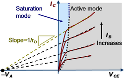
The output resistance, usually denoted by rO, is a measure of how much collector-base voltage change is necessary to cause a given change in transistor output current when the transistor is in active mode. The reason a change in VCB changes the current is that the width of the neutral base region, where the current is governed by the gradient in carrier density, is narrowed when the CB junction becomes more reverse biased. Therefore the gradient of the carrier density , which is the difference between the high density near the emitter and the low density near the collector divided by the neutral base width, is increased with increased reverse bias of the CB junction. This phenomenon is called either base-width modulation or the Early effect.[6] According to a simple empirical model (see the figure), the output resistance is given by:
where VA is called the Early voltage, and is a parameter entering most models of the transistor. The current IC(IB, VCE) is the collector current evaluated at the selected base current and the selected voltage VCE. The voltage VCE is used instead of VCB because the output resistance is connected between the collector and the emitter in the hybrid-pi model (discussed in the section on frequency dependence below), which is convenient but physically unmotivated. Inasmuch as VBE is relatively small and does not change much, the difference between the CB voltage and the CE voltage in this definition is a minor point.
The figure shows the slope of the output current as 1/rO, and indicates how it increases (how rO decreases, as suggested by the formula) as the collector current increases.
A simplified model for the DC current-voltage relations for the bipolar in active mode including the Early effect is then:[7]
- Failed to parse (SVG (MathML can be enabled via browser plugin): Invalid response ("Math extension cannot connect to Restbase.") from server "https://wikimedia.org/api/rest_v1/":): {\displaystyle i_B=\frac{I_S}{\beta_0}\left( e^\left(v_{BE}/V_{th}\right)-1\right) \ ,}
- Failed to parse (SVG (MathML can be enabled via browser plugin): Invalid response ("Math extension cannot connect to Restbase.") from server "https://wikimedia.org/api/rest_v1/":): {\displaystyle \beta=\beta_0 \left(1+\frac{v_{CE}}{V_A}\right) \ ,}
- Failed to parse (SVG (MathML can be enabled via browser plugin): Invalid response ("Math extension cannot connect to Restbase.") from server "https://wikimedia.org/api/rest_v1/":): {\displaystyle i_C=\beta i_B = I_S\left(e^\left(v_{BE}/V_{th}\right)-1\right)\left(1+\frac{v_{CE}}{V_A}\right ) \ , }
where β0 is the value of β extrapolated to VCE=0, Vth is the thermal voltage already mentioned, and IS is a parameter that varies from device to device called the saturation current. The base current expression is the simple diode law for the EB junction.
Frequency dependence

Collector current level dependence of transition frequency in a Si-Ge HBT.[8]
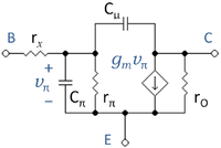
Another important device quality is its speed of response to transient signals. The bipolar transistor is a very non-linear device, so its transient response for large signals requires a numerical calculation. However, some idea is gained using a small-signal model and treating the device for small variations about a quiescent condition (its Q-point). Such a circuit is shown in the figure for a device biased in active mode, the hybrid-pi model. This circuit reduces the problem of frequency response to the RC time-constants related to charge and discharge of various capacitances through their associated resistors.
To boil down the frequency response to a single number (admittedly a limited summary of merit) the so-called transition frequency, denoted fT or ft, is used. This frequency is found by examination of the short-circuit current gain of the transistor, which can be estimated using the hybrid-pi model in common-emitter configuration. With a small-signal current applied to the base and the collector short-circuited to the emitter, which is grounded, the current flowing into the transistor through the collector is:
- Failed to parse (SVG (MathML can be enabled via browser plugin): Invalid response ("Math extension cannot connect to Restbase.") from server "https://wikimedia.org/api/rest_v1/":): {\displaystyle i_c = \left( g_m -j\omega C_\mu \right ) v_\pi \ , }
while the signal current is related to the input voltage vπ by:
- Failed to parse (SVG (MathML can be enabled via browser plugin): Invalid response ("Math extension cannot connect to Restbase.") from server "https://wikimedia.org/api/rest_v1/":): {\displaystyle i_s = \left( j\omega(C_\pi+C_\mu) +1/r_\pi \right)v_\pi \ . }
The current gain is accordingly:
- Failed to parse (SVG (MathML can be enabled via browser plugin): Invalid response ("Math extension cannot connect to Restbase.") from server "https://wikimedia.org/api/rest_v1/":): {\displaystyle \frac{i_c}{i_s} = \frac{g_m-j\omega C_\mu}{j\omega (C_\pi+C_\mu) +1/r_\pi} = \frac{g_m r_\pi - j\omega C_\mu r_\pi}{1+j\omega(C_\pi+C_\mu)r_\pi} \ . }
If we invoke the relation:
- Failed to parse (SVG (MathML can be enabled via browser plugin): Invalid response ("Math extension cannot connect to Restbase.") from server "https://wikimedia.org/api/rest_v1/":): {\displaystyle g_m r_\pi = \frac{I_C}{V_{th}} \ \frac {V_{th}}{I_B} = \frac{I_C}{I_B} = \beta \ , }
with Vth the thermal voltage and IC, IB the DC bias collector and base currents, then:
- Failed to parse (SVG (MathML can be enabled via browser plugin): Invalid response ("Math extension cannot connect to Restbase.") from server "https://wikimedia.org/api/rest_v1/":): {\displaystyle \frac{i_c}{i_s} = \frac{\beta - j\omega C_\mu r_\pi}{1+j\omega(C_\pi+C_\mu)r_\pi} \ , }
which, of course, provides the zero-frequency current gain of the transistor as β. However, as frequency increases the current gain drops once the corner frequency is passed, f > fC:
- Failed to parse (SVG (MathML can be enabled via browser plugin): Invalid response ("Math extension cannot connect to Restbase.") from server "https://wikimedia.org/api/rest_v1/":): {\displaystyle f_C = \frac{1}{2\pi (C_\pi+C_\mu )r_\pi} \ . }
The transition frequency denoted fT is defined as the frequency where the current gain rolls off to a value of unity:
- Failed to parse (SVG (MathML can be enabled via browser plugin): Invalid response ("Math extension cannot connect to Restbase.") from server "https://wikimedia.org/api/rest_v1/":): {\displaystyle \left|\frac{i_c}{i_s}\right| =1 = \left|\frac{\beta}{1+jf_T/f_C}\right| \ , }
or
- Failed to parse (SVG (MathML can be enabled via browser plugin): Invalid response ("Math extension cannot connect to Restbase.") from server "https://wikimedia.org/api/rest_v1/":): {\displaystyle f_T \approx \beta f_C = \frac{g_m}{2\pi (C_\pi+C_\mu)} \ . }
In active mode, capacitance Cμ is the depletion capacitance of the CB junction, which is a lightly doped junction with a large depletion layer width. Thus, this capacitance is small, say 2 pF. On the other hand, Cπ includes the heavily doped EB junction capacitance and the very large diffusion capacitance due to the injected electrons, and is typically several hundred pF. That is the justification for the rather cavalier brushing aside of the frequency dependence in the numerator, jωCμrπ. The frequency dependence in the denominator depending upon Cπrπ will dominate any effect of the numerator introduced by Cμrπ.
Both the transconductance gm and the diffusion capacitance in Cπ are dependent upon the collector current density, so it is expected that the transition frequency will vary with current, and current dependence is observed, as shown in the figure. Initially fT increases because of the dominance of gm, but eventually one expects saturation as denominator and numerator both become proportional to current density. In fact, however, at high current density the transition frequency begins to decline, one of many non-ideal high injection effects.
References
- ↑ WS Shockley (1976). "The path to the conception of the junction transistor". IEEE Trans Electron Dev. ED-23: pp. 597 ff.
- ↑ M Riordan & L Hoddeson (1997). Crystal fire: the birth of the information age. W. W. Norton & Company. ISBN 0393041247.
- ↑ C. K. Maiti, G. A. Armstrong (2001). “Principle of SiGe HBTs”, Applications of silicon-germanium heterostructure devices. CRC Press, pp. 77 ff. ISBN 0750307234.
- ↑ AG Baca et al, (2000). “DC and microwave characteristics of 100V GaAs/AlGaAs HBTs”, Compound semiconductor power transistors II: proceedings of the thirty second international symposium. Electrochemical Society; Electronics Division, p. 131. ISBN 1566772664.
- ↑ Named after Hermann K Gummel, from Bell Laboratories, a pioneer in numerical modeling of the bipolar transistor and an author of the Gummel-Poon model much used for the bipolar transistor.
- ↑ The Early effect is named after James M. Early, one of the Bell Laboratories scientists involved in the development of the bipolar transistor.
- ↑ Richard C Jaeger (1997). “§5.12: The Early effect and Early voltage”, Microelectronic circuit design. McGraw-Hill, 196 ff. ISBN 0-07-114386-6. These equations do not include things like the current dependence of β, and are intended to be only qualitative.
- ↑ Based upon Figure 5.5 in John D. Cressler, Guofu Niu (2003). Silicon-germanium heterojunction bipolar transistors. Artech House, p. 148. ISBN 1580533612.


